Introduction
Digital electronics is probably the most impactful and widespread technology now. It forms the basis of all of the chips- from ARM microcontrollers to processors in cellphones, all the way to uberpowerful AMD Threadrippers. In all these cases, digital electronics reign supreme.
It is very useful to learn not only about basic principles but also how these principles and the components of Digital Electronics exactly form the basis of the modern world, i.e., how do we go from basic logic gates to fully functional computers.
Elements of Computing Systems
Digital Electronics is not only important because it is the base of the modern technology that literally governs our lives, but it makes us better as programmers, and computer scientists.
Whether we are self-taught programmers or a person with a 4-year CS degree, we were never taught how we go from basic logic gates to CPUs.
A book that I have come across- The Elements of Computing Systems by By Noam Nisan and Shimon Schocken does just that. It teaches you how the basic building blocks of modern computers actually create the computers.

[Although it shows the new 2nd edition, I am reading the first one]
It promises to teach you, actively, how we can start from nothing but a NAND gate and go all the way to a full-fledged computer with an operating system, and a general-purpose programming language that runs on it, which can be used to create anything. The book is also known as nand2tetris.
I have started reading this book and working through it every Sunday, and I have almost finished a chapter.
Building Gates from Elementary Gates
People who have taken a Digital Architecture class or a Digital Electronics class will know that NAND (NOT AND) gates are called “universal gates” because some combination of them are able to create any other gates. So, when you have a NAND gate with you, you can create a general-purpose computer with it. And the book makes you do that. It makes you create many logic gates starting from AND, NOT, and OR with nothing but a pre-implemented NAND gate.
So, a NAND gate is already implemented and supplied. You first have to create AND, OR, and NOT gates. Then you go on to further create XOR gates, Multiplexors (MUX), Demultiplexors (D-MUX), and multi-bit versions of these gates and basic gates with what you have built previously, viz. AND, OR, NOT, and NAND gates.
This is a fascinating task in itself, and very intellectually stimulating.
This is where the core of the post comes in.
I will show you how to implement any Boolean function with nothing but three logic gates. This is a trick worth knowing.
Let’s start.
Implementing a Boolean Function
Design a Boolean Function
Let’s say we need a Boolean function that behaves in such a way-
| A | B | C | Y |
|---|---|---|---|
| 0 | 0 | 0 | 1 |
| 0 | 0 | 1 | 0 |
| 0 | 1 | 0 | 0 |
| 0 | 1 | 1 | 0 |
| 1 | 0 | 0 | 1 |
| 1 | 0 | 1 | 1 |
| 1 | 1 | 0 | 1 |
| 1 | 1 | 1 | 0 |
This truth table tells you that we need such a Boolean function that outputs 1 iff- * A, B, and C, three Boolean variables, are all 0 * only A is 1, B and C are 0 * A and C are 1, B is 0 * A and B are 1, C is 0
Now, in some situations, you might need to define a Boolean function that behaves as you expect. Do not worry about what this function is doing. Let’s focus on the implementation part.
Boolean Expression
I am assuming that you already know about the basic gates, and how they function.
So, in the first step to build a Boolean function, you must create the Boolean expression. Just like a Boolean variable can have two values (0, 1), and a Boolean function can only output two values (0, 1, duh!), a Boolean expression always evaluates to either 0 or 1.
How to actually do it?
- You should just note in which cases the function outputs a 1. Focus just on those.
- Note which variables are on (1) and which are off (0).
- Keep the variables unchanged which are 1 in this case, and take a negation of those which are off (in electronics, you would put them through NOT).
- Multiply them together.
- For these products for each 1 in the output, just add them together.
That’s it. You have got your Boolean expression.
Let me go through it step by step.
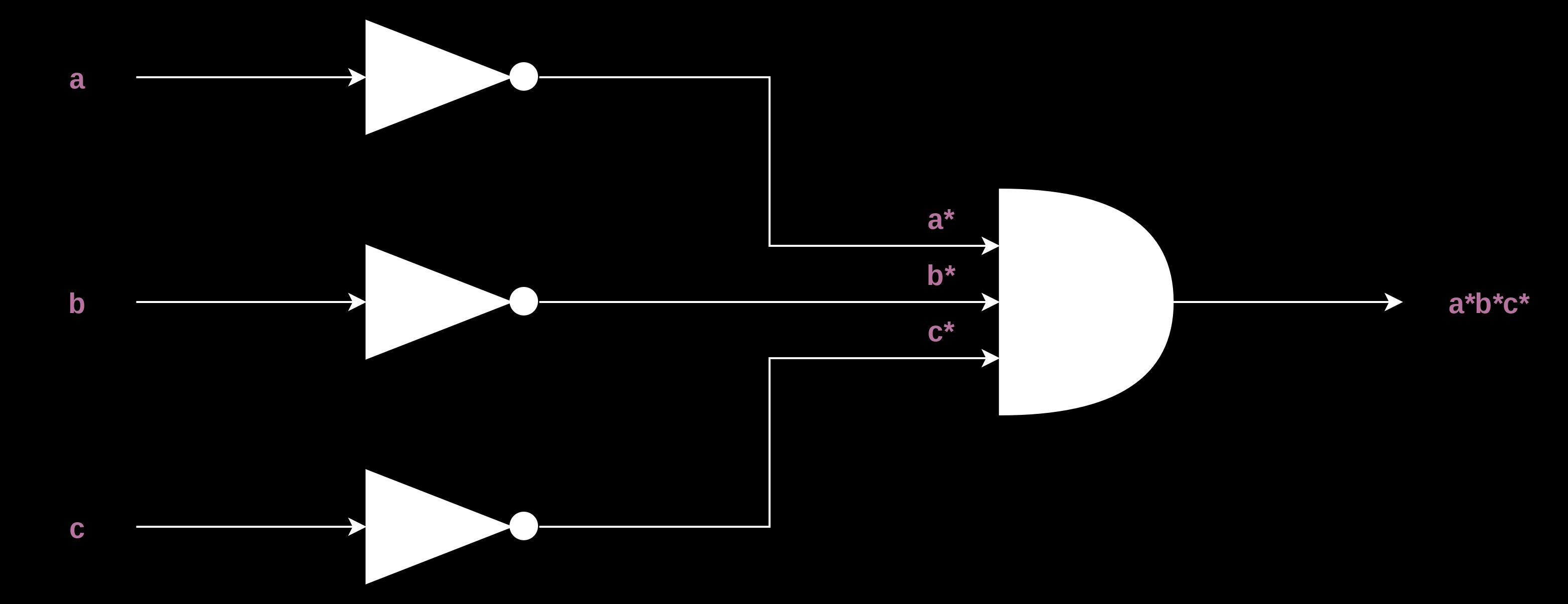
In the first occurrence of 1 in the output, we see that all the input variables are off. So, we get a*, b*, and c*, where a, b, and c are the variables representing inputs A, B, and C, respectively, and x* is the negation of x. We multiply them together, and we get a*b*c*.
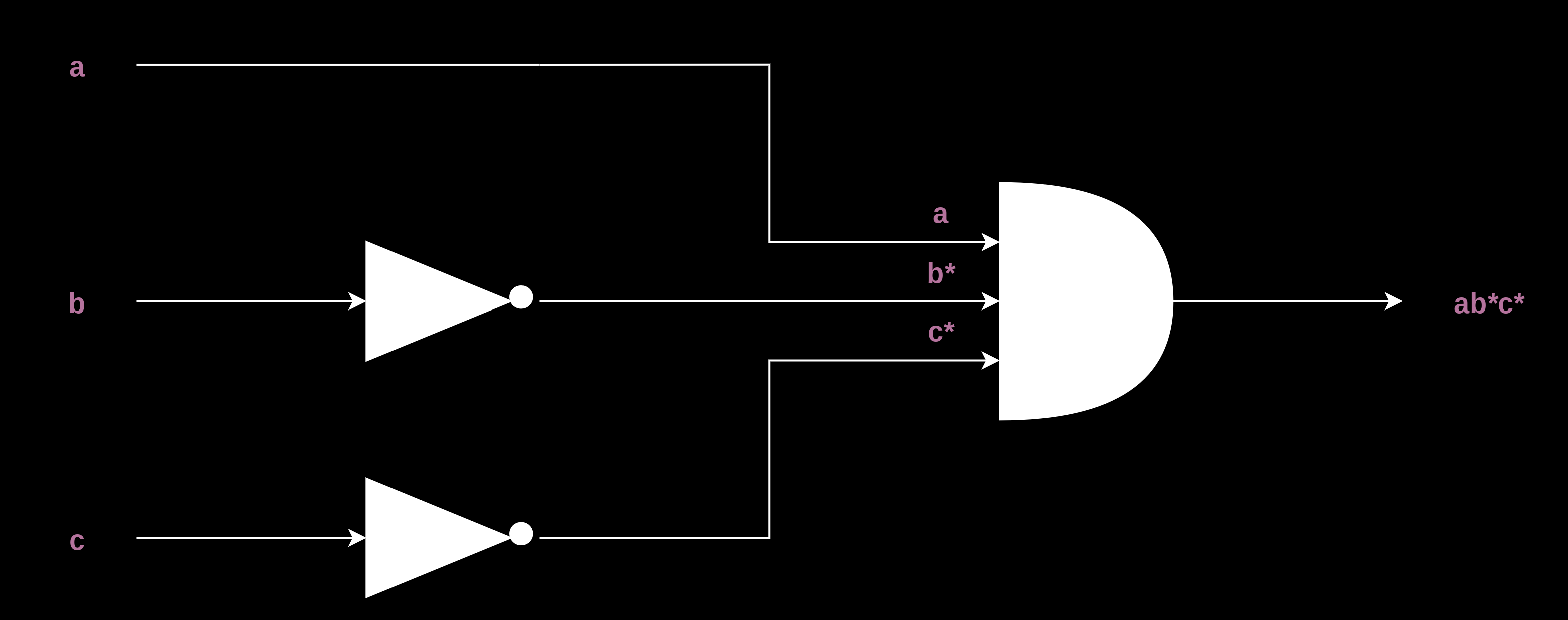
In the second occurrence of 1, in a similar manner, we get- ab*c*.
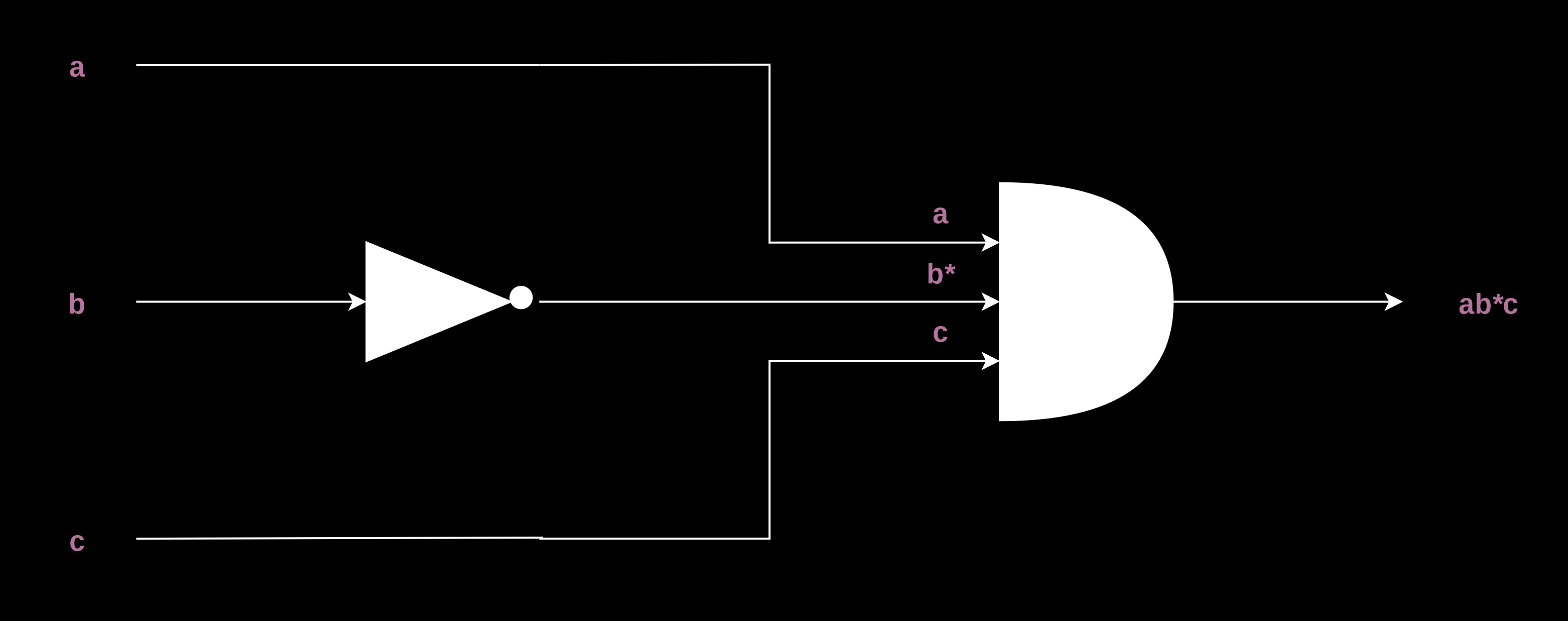
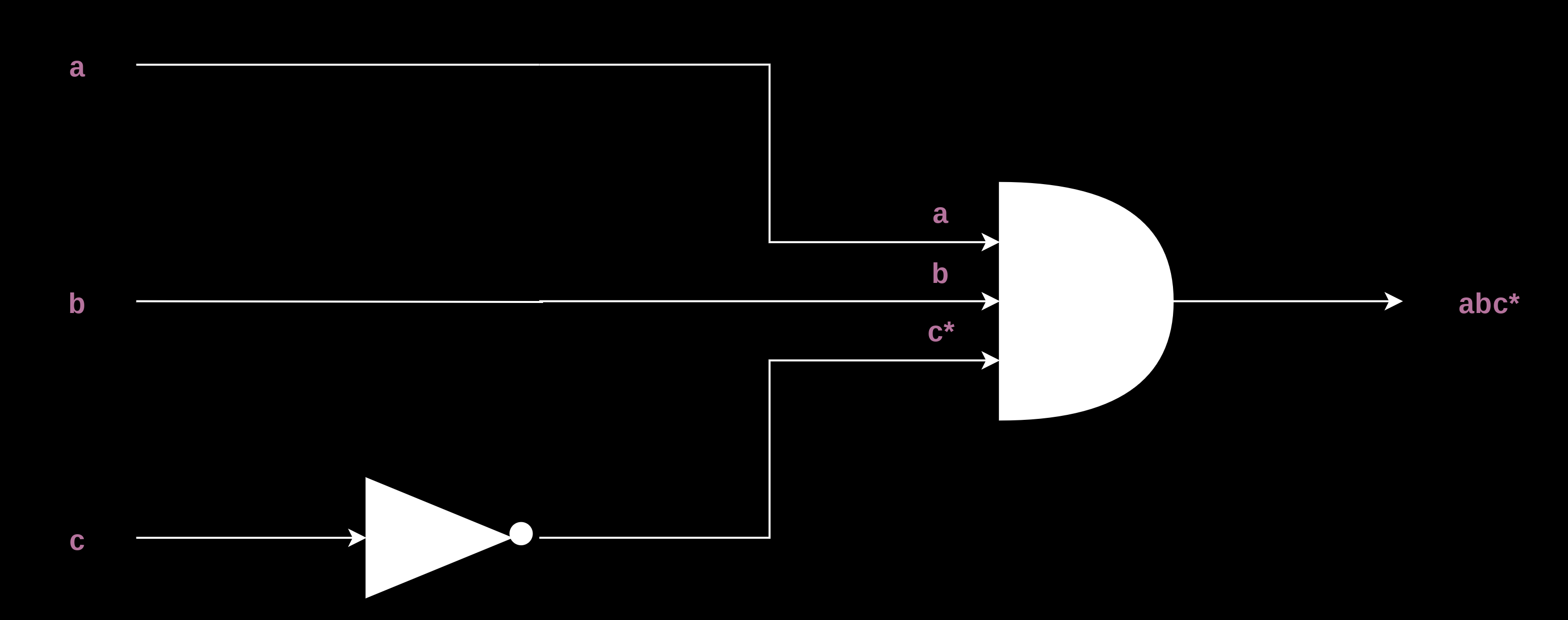
For the third and fourth occurrences of 1, we get ab*c, and abc*, respectively.
We have to add them. And doing so, we get-
\[ y = \overline{a}\overline{b}\overline{c} + a\overline{b}\overline{c} + a\overline{b}c + ab\overline{c} \]
[You are required to write cases in the proper order. The first of three variable has these values row-wise- 0-0-0-0-1-1-1-1, the second one varies- 0-0-1-1-0-0-1-1, and the third one- 0-1-0-1-0-1-0-1.]
Implementation
You might be already aware that negation is passing through a NOT gate, multiplying is just passing through an AND gate, and adding is just an OR gate.
The first component a*b*c* can be obtained in this way-
And here are the second, third, and fourth components-
And,
Now, we have to add them all together, i.e. put these components through an OR gate. The output of the OR gate will be our final output.
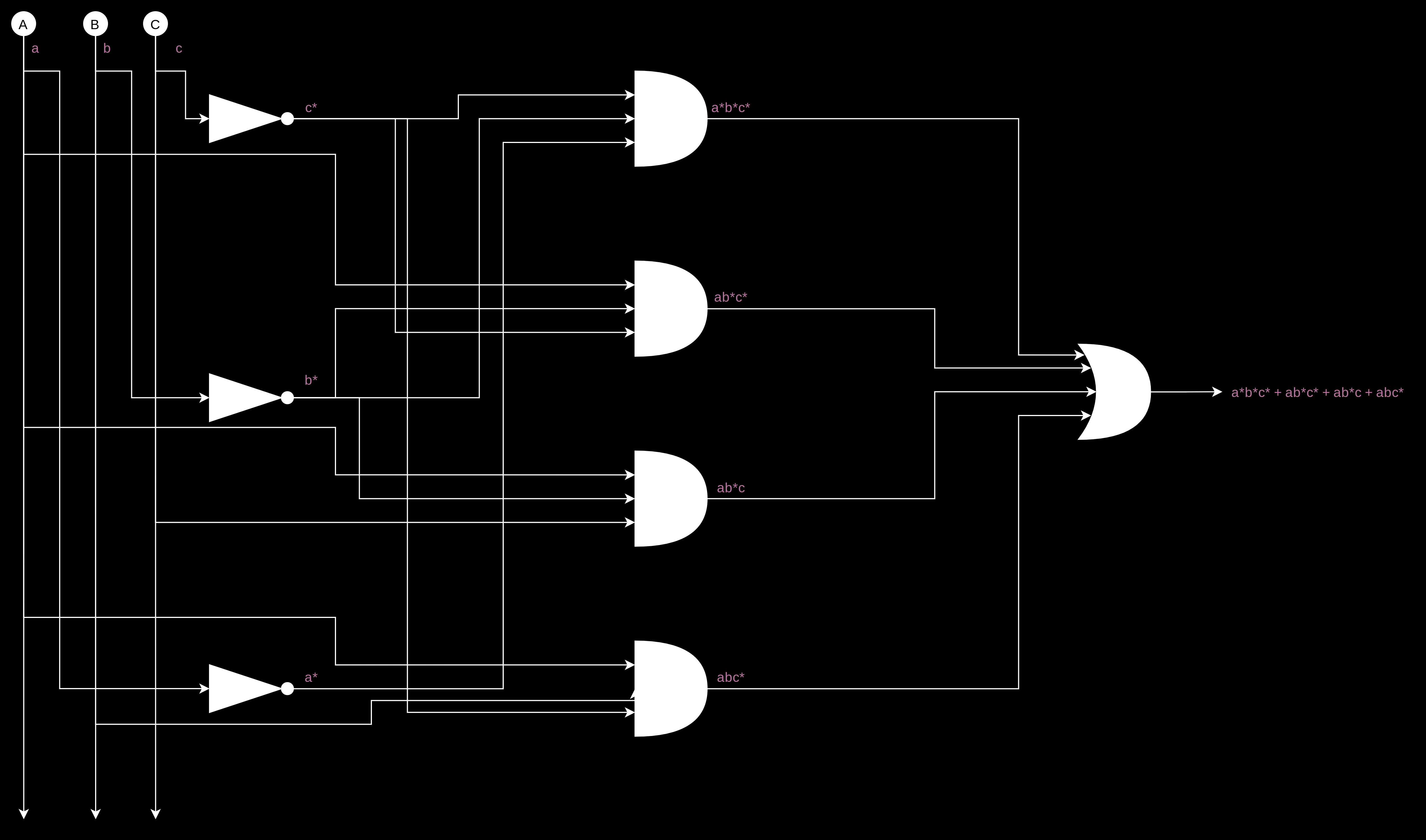
Our final output.
HDL: Implement and Test
Now, if you have ICs lying around, you can quickly test this with a power supply or a 5V cell, and some wires. You will also need a multimeter or LED bulbs to check your output.
But, remember, we are building a computer from scratch when following this book. Using thousands of ICs to build a computer is not slightly practical unless you happen to have a contract with TSMC!
Something called HDL (Hardware Description Language) is used. It is an intuitive, high-level, special-purpose programming language that you use to design and test chips, and use previously created chips.
It is implemented in Java, but you do not have to worry about its implementation, you just need to use it. A GUI program is also supplied to do load and test chips.
For example, given a NAND gate, you will design an AND gate this way.
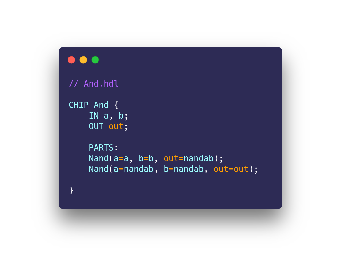
As you can see, it is very intuitive, and you can pick it up in 20 minutes.
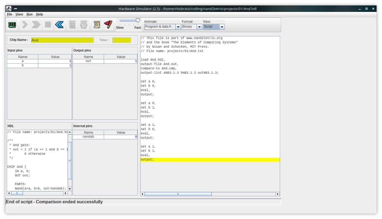
And, this is how you’d test this:
To write our custom function in HDL, we would do-
// Custom.hdl
// this is a part of Hashnode blog Convoluted demo

CHIP Custom {
    IN a, b, c;
    OUT out;

    PARTS:
    Not(in=a, out=nota);
    Not(in=b, out=notb);
    Not(in=c, out=notc);
    And(a=nota, b=notb, out=notanotb);
    And(a=notanotb, b=notc, out=w1);
    And(a=a, b=notb, out=anotb);
    And(a=anotb, b=notc, out=w2);
    And(a=anotb, b=c, out=w3);
    And(a=a, b=b, out=ab);
    And(a=ab, b=notc, out=w4);
    Or8Way(in[0]=w1, in[1]=w2, in[2]=w3, in[3]=w4, out=out);
}
And as this is a custom chip, the .tst test file, and .cmp compare file are not supplied. So, for testing this chip, I wrote my own.
Here is the test (.tst) file-
// Custom.tst
// test file for testing custom chip
// could be found at- https://gist.github.com/ghosh-r/c4e6f5ceb1e7ea2e3ba3601c9de121be

// test file for a custom chip in Convoluted, a Hashnode blog

load Custom.hdl,
output-file Custom.out,
compare-to Custom.cmp,
output-list a%B3.1.3 b%B3.1.3 c%B3.1.3 out%B3.1.3;

set a 0,
set b 0,
set c 0,
eval,
output;

set a 0,
set b 0,
set c 1,
eval,
output;

set a 0,
set b 1,
set c 0,
eval,
output;

set a 0,
set b 1,
set c 1,
eval,
output;

set a 1,
set b 0,
set c 0,
eval,
output;

set a 1,
set b 0,
set c 1,
eval,
output;

set a 1,
set b 1,
set c 0,
eval,
output;

set a 1,
set b 1,
set c 1,
eval,
output;
And here is the compare (.cmp) file. It contains the truth table that we expect.
// Custom.cmp
// compare file for chip Custom.hdl
// found at- https://gist.github.com/ghosh-r/c4e6f5ceb1e7ea2e3ba3601c9de121be
// test file at- https://gist.github.com/ghosh-r/cef52b9f6ac017e00d64460b025a53fe

|   a   |   b   |   c   |  out  |
|   0   |   0   |   0   |   1   |
|   0   |   0   |   1   |   0   |
|   0   |   1   |   0   |   0   |
|   0   |   1   |   1   |   0   |
|   1   |   0   |   0   |   1   |
|   1   |   0   |   1   |   1   |
|   1   |   1   |   0   |   1   |
|   1   |   1   |   1   |   0   |
Note that the text in Compare files is not robust to whitespaces.
It will be compared with the output file generated by the simulator.
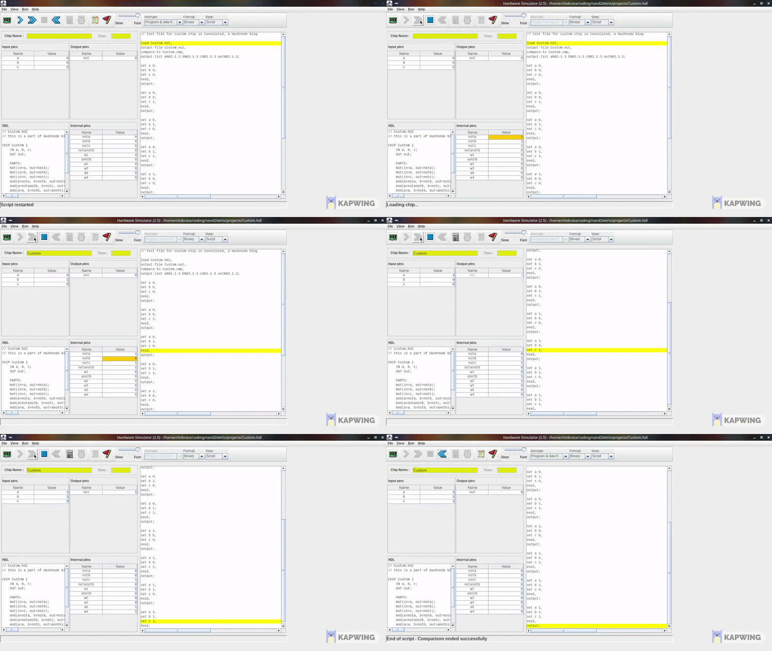
Here’s how the successful run looks like-
Another Example: XOR Gate
Suppose you want to implement a XOR gate from basic gates. And the truth-table would be-
| A | B | Y |
|---|---|---|
| 0 | 0 | 0 |
| 0 | 1 | 1 |
| 1 | 0 | 1 |
| 1 | 1 | 0 |
This will be your Boolean expression-
\[ y = \overline{a}b + a\overline{b} \]
And this will be your HDL implementation.
// Xor.hdl

CHIP Xor {
    IN a, b;
    OUT out;

    PARTS:
    Not(in=a, out=nota);
    Not(in=b, out=notb);
    And(a=a, b=notb, out=w1);
    And(a=nota, b=b, out=w2);
    Or(a=w1, b=w2, out=out);
}
Conclusion
I showed you how to implement any Boolean function with nothing but three elementary logic gates. However, you should keep in mind that this approach is impractical when there are more variables, and the chip you want is more complicated.
Follow the blog to get more similar posts.